Printed Circuit Board Drawing
Printed Circuit Board Drawing - You should ensure the circuit is mirrored before doing that (most pcb layout programs have this as an option when printing). Web to design a printed circuit board (pcb), you need to draw holes, pads, and wires for your circuit. Schematic capture to create the circuitry connectivity in a diagram and then pcb layout to design the actual physical circuit board. The printed circuit board of the host must ensure that the antenna clearance area meets the antenna specifications. Web a printed circuit board (pcb) layout is the blueprint that guides the production of circuit boards which are the backbone of any electronic device. Pcb design is broken into two main categories: Welcome to our detailed guide on printed circuit board basics: What is a printed circuit board? Read on to learn the universal pcb design steps. Web printed circuit boards are also known (some would say, more correctly known) as printed wiring boards, or simply printed boards. Nets are the traces on the board. If you are into electronics, pcbs are some of the most common things you will see. But we will settle on the more common term pcb for this article. In the picture above, there are traces that electrically connect the various connectors and components to each other. Web to design a printed circuit. This is accomplished using pcb circuit board design cad tools. Web pcb is an acronym for printed circuit board. We can accept just about any standard format for your fabrication notes. It is suggested that putting the antenna in the corner of. Production in shanghai started in 2002. Web pcb is an acronym for printed circuit board. Web printed circuit boards, also known as printed wiring cards or printed wiring boards, are boards with lines and pads connecting various points together. In the picture above, there are traces that electrically connect the various connectors and components to each other. Web pcb fabrication drawing/fab print. Welcome to our detailed. Web printed circuit board design begins with the creation of a conceptual block diagram. A pcb allows signals and power to be routed between physical devices. In a pcb, individual traces electrically connect the various components and connectors together, the pcb allowing signal and power routing between physical devices. Web at&s has been present in china for more than 20 years. Web printed circuit boards are also known (some would say, more correctly known) as printed wiring boards, or simply printed boards. Once printed, make sure you don’t touch the ink part on the paper as it can get on your hands. But while it’s important to keep in mind who you’re working with, here are some basic elements that are common to most printed circuit board fabrication drawings to. It shows the layout of the components, their connections, and how they work together to perform a specific function. In the picture above, there are traces that electrically connect the various connectors and components to each other. Think of a pcb as a physical canvas or road map for designing electronic circuits. This article explores the core principles of pcb layout, component placement, trace routing, signal integrity, and more. Understanding the basic concepts and terminology related to pcb design is essential for creating reliable and efficient electronic products. Nets are the traces on the board. This software just lets you develop electronics the right way. Web printed circuit board (pcb) design involves the creation of a layout that defines the electrical connections and mechanical structure of an electronic device. It provides a stable and conductive pathway for electrical currents to flow across a layer from one net to another, passing through plated holes to internal layers or the opposing side, allowing various components to interact with one.
Printed Circuit Board Vector 338569 Vector Art at Vecteezy
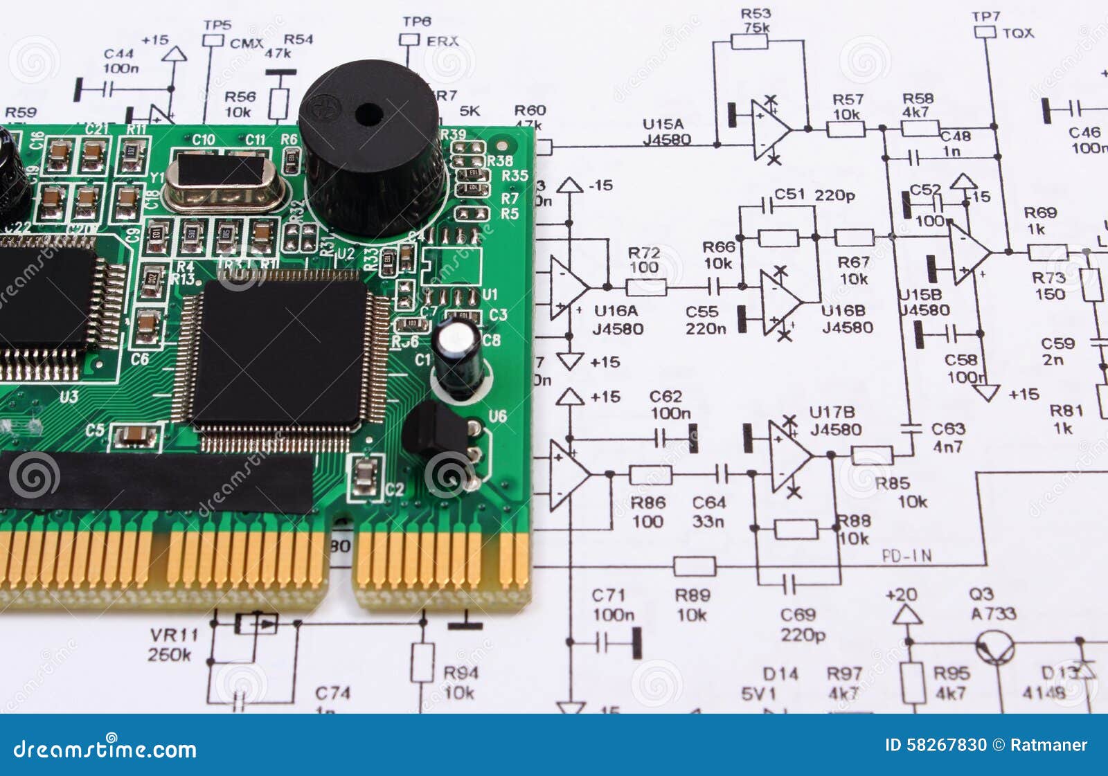
Printed Circuit Board Lying on Diagram of Electronics, Technology Stock

Printed Circuit Board Design, Diagram and Assembly Steps & Tutorial
Web Make Sure That During Your Printed Circuit Board Design Process You Are Communicating With Your Manufacturer To Know What They Need In Their Assembly Drawings.
A Simple Readme.txt Works Just As Well.
The Printed Circuit Board Of The Host Must Ensure That The Antenna Clearance Area Meets The Antenna Specifications.
The Process Of Moving, Mixing And Generation Of Droplets Was Demonstrated.the Minimum Voltage In Need Was About 20 V And A Velocity Of Up To 96 Mm/S Was Achieved.
Related Post: