Pcb Drawing
Pcb Drawing - Overall best pcb design software on windows, most popular among professionals. Web make your first printed circuit board. Web published date july 20, 2022. The schematic symbols in the easyeda library already have footprints associated with them, but they can be changed if your’re using a different size. Web the pcb footprint will define the component’s physical dimensions and placement of the copper pads or through holes. Learn to create electronic components. First, you need to install a pcb design software. 1:37 min.) what is autodesk fusion? It's so fundamental that people often forget to explain what a pcb is. Easyeda is a free and easy to use circuit design, circuit simulator and pcb design that runs in your web browser. First, you need to install a pcb design software. Download my guide with all the steps you need to design your first printed circuit board (pcb) from scratch. Web free online pcb cad library | ultra librarian. Popular fab print file types we can use are: Web 9:00 am to 4:00 pm pt. This is a free pcb design tool unlike anything you’ve seen before. Web circuitmaker is schematic and pcb design software that is built upon altium designer technology. Then it’s time to put your problem solving skills to the test by placing electrical components within a tightly constrained space. Defining two major concepts of board design and production: First, you need. Web the pcb design process begins by converting an electronics schematic diagram into a physical circuit board layout. Best of all, it's free to use. This tutorial will breakdown what makes up a pcb and some of the common terms used in the pcb world. Web free online pcb cad library | ultra librarian. This software just lets you develop. Defining two major concepts of board design and production: Create and review schematics based on engineering requirements. Easyeda is a free and easy to use circuit design, circuit simulator and pcb design that runs in your web browser. Now is a good time to decide which components you’ll be using. Or browse intelligent reference designs like pmp40988. A pcb schematic is a logical and visual representation of an electrical circuit. This tutorial will breakdown what makes up a pcb and some of the common terms used in the pcb world. Printed circuit board (pcb) design and layout is both an art and a science, and it can be difficult to get started designing a new circuit board from scratch. Web pcb fabrication drawing/fab print. Pressure sensor, max17690ate+t, or 1mm connector. Overall best pcb design software on windows, most popular among professionals. Use schematic capture, create pcb designs and view them in 3d, all forever free. This software just lets you develop electronics the. Web the pcb footprint will define the component’s physical dimensions and placement of the copper pads or through holes. I highly recommend kicad for making your pcb. The schematic symbols in the easyeda library already have footprints associated with them, but they can be changed if your’re using a different size.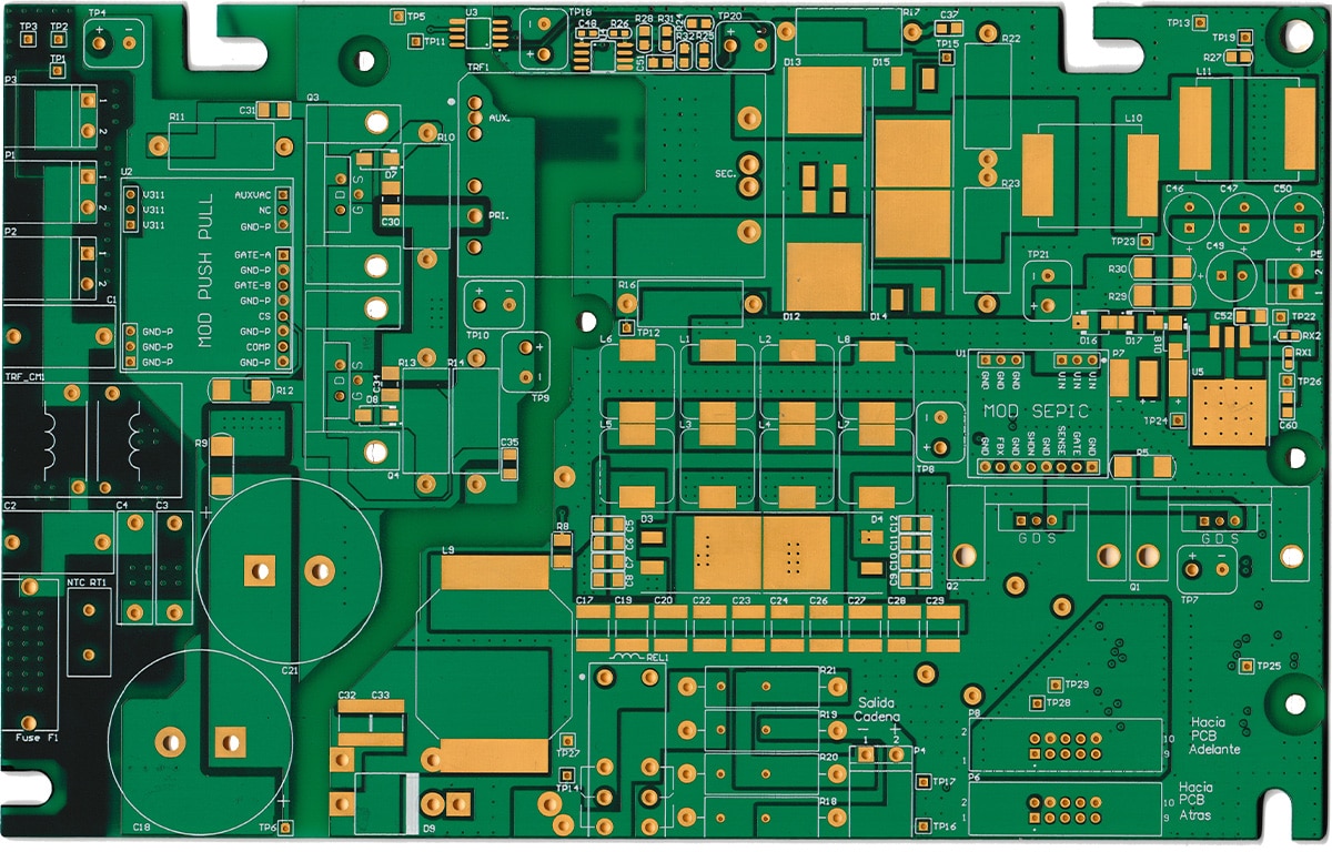
Custom PCB Design Gallery for double & multilayer boards

Free PCB Schematic Entry & Layout Software Beat Eagle for Some Features

Printed Circuit Board Design, Diagram, Assembly Steps, Tutorial
Web One Of The Key Concepts In Electronics Is The Printed Circuit Board Or Pcb.
Access Free Symbols, Footprints, And 3D Models From The World’s Largest Cad Library.
Create A Blank Pcb, Build The Stackup, And Create Design Rules.
The World’s Most Trusted Pcb Design System.
Related Post: